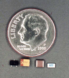
Figure 1. An ordinary dime dwarfs typical SMD components. From left to right: SOT-23 bipolar transistor, 2.2 mfd tantalum capacitor, ceramic capacitor, and 82-Ohm resistor.
Introduction
Surface mount devices (SMDs) are used in a growing number of commercial and industrial products. Due to their small size (see Figure 1), prototype manufacturing, rework, and repair can be difficult and are best performed using specialized techniques specific to this technology. Learning these techniques will help you succeed when working with these small components.
Why Use Surface Mount Technology?
SMDs have improved performance over through-hole components due to their smaller size, shorter internal leads, and smaller board layouts. These factors reduce the circuit’s parasitic inductance and capacitance. SMDs can also be more cost effective than traditional through-hole components due to the smaller board size, fewer board layers, and fewer holes.
SMDs can also be easier to replace than through-hole components on multilayer boards. This is because it is very difficult to heat the long hole on a multilayer board, but much easier to heat just the pad and component terminal of an SMD on the surface of a board.
This article is for those technicians and small manufacturers who would like to learn about and experiment with SMDs, yet do not initially have access to professional SMD rework stations, solder pastes, hot air jets, or illuminated magnifiers. SMDs can be challenging to solder, so it is best to learn general soldering skills on larger components before attempting to work with SMDs.
The methods presented here are not the only ones available. SMD components can be worked with in many different ways (just as through-hole components). The goal of this paper is simply to give a quick introduction to several methods that the small manufacturer or professional technician can use to successfully work with this technology.
SMD Safety Precautions
Surface mount components are very small, and therefore special precautions (in additional to those required when working with through-hole components) must be taken:
Do not eat or drink when working with surface mount components
Do not use cups, plates, or any food related items to hold or store surface mount components
Keep surface mount components away from children and pets
Always wear safety goggles
Work away from the edge of a desk or workbench to insure that components will not fall on the floor
Keep a strong light and magnet available to search for components that have dropped on the floor
The Work Area
Because SMDs are very small, it is important to make them "look" bigger. This can be accomplished by illuminating the work surface with a very bright light. To illustrate this effect, take some difficult-to-read fine print (like on the back of a credit card application) and try reading it in a dimly lit room, then try reading it a few inches from a bright desk lamp. The difference is dramatic.
A swing-arm desk lamp with a 100-watt frosted bulb positioned close to the work surface works very well. The lamp should be adjustable from 6 to 24 inches above the desktop. Regular room lighting or shop lights just are not bright enough. It is also helpful to set up the lamp so it can be swung over the edge of the desk and illuminate the floor. This helps with finding dropped components.
The second trick is to work on an absolutely clean, bright white surface. The SMD work tray shown in Figure 2 works very well. The white paper gives contrast to the components, and the small sides help prevent the SMDs from getting lost.
To build the SMD work tray, start by removing the cardboard back from a 8 ½" x 11" writing tablet. On one side, glue two sheets of bright white copy paper using rubber cement. Two sheets are necessary because the paper is not completely opaque. When the glue has dried, flip it over and draw a box ½ inches from all four sides. Bend the cardboard at the lines, forming a 7 ½" x 10" tray. Fold up each corner. Glue the corners together using white glue. Clamp each corner using a clothespin until the
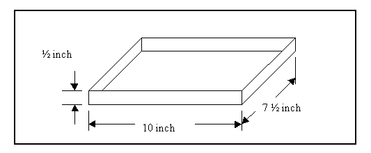
Figure 2. The SMD work tray. Line the inside with several layers of high-brightness white copy paper. Glue all edges and corners so components cannot slip underneath. Base material is the back of a 8 ½ inch x 11 inch writing tablet.
You will be amazed how much of a difference a bright light and white work surface will make when working with these components.
Tools and Equipment
The tools and equipment you will need are shown in the sidebar. Self-locking tweezers (Figure 3) cost only a few dollars (available from S. LaRose Inc., 1-888-752-7673, www.slarose.com) and work much better than regular tweezers. Vacuum pick-up tools can also be used, but are considerably more expensive. Select a low wattage (15 or 25 watt) or temperature controlled (600F) pencil soldering iron with a pointed tip.
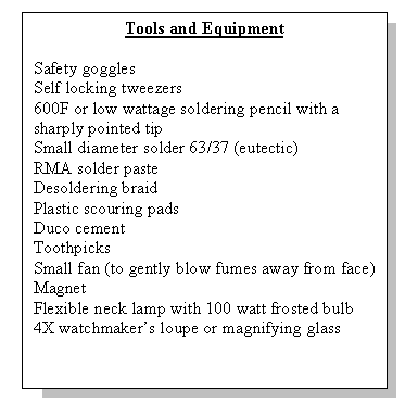
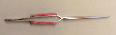
Figure 3. Self-locking tweezers help position SMT components.
To clean the circuit board before soldering you will need a nonconductive abrasive pad. Don’t use steel wool or a steel wool scouring pad, since they may leave small (almost microscopic) steel wires behind. A strong magnet is useful for finding dropped components. You will also need a 4X watchmakers loupe or magnifying glass. Use this to read the component markings on chip resistors and electrolytic capacitors.
Identifying SMDs
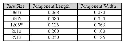
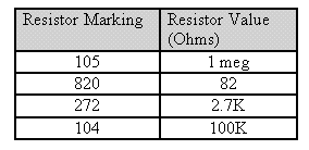
The general shape of some common SMDs are shown in Table 1. Note that many components (like chip capacitors) are not routinely labeled. This is why the SMD test tweezers (http://poeth.com/SMD.htm) are so useful. Typical case sizes for chip resistors and capacitors are listed in Table 2. To find the approximate size, multiply the first two digits by 10 to get the length in mils, and multiply the last two digits by 10 to get the width in mils. The most common size for chip resistors and chip capacitors is 1206.Resistors are frequently marked with a three-digit number, and some typical values are shown in Table 3. The first two numbers are the significant digits of the value, and the last digit is the multiplier (the number of zeros to add to the first two digits). For example, a chip resistor labeled 102 has a value of 1000 Ohms, or 1K Ohms.
Figure 3. Self-locking tweezers help position SMT components.
To clean the circuit board before soldering you will need a nonconductive abrasive pad. Don’t use steel wool or a steel wool scouring pad, since they may leave small (almost microscopic) steel wires behind. A strong magnet is useful for finding dropped components. You will also need a 4X watchmakers loupe or magnifying glass. Use this to read the component markings on chip resistors and electrolytic capacitors.
Identifying SMDs
The general shape of some common SMDs are shown in Table 1. Note that many components (like chip capacitors) are not routinely labeled. This is why the SMD test tweezers (http://poeth.com/SMD.htm) are so useful. Typical case sizes for chip resistors and capacitors are listed in Table 2. To find the approximate size, multiply the first two digits by 10 to get the length in mils, and multiply the last two digits by 10 to get the width in mils. The most common size for chip resistors and chip capacitors is 1206.Resistors are frequently marked with a three-digit number, and some typical values are shown in Table 3. The first two numbers are the significant digits of the value, and the last digit is the multiplier (the number of zeros to add to the first two digits). For example, a chip resistor labeled 102 has a value of 1000 Ohms, or 1K Ohms.
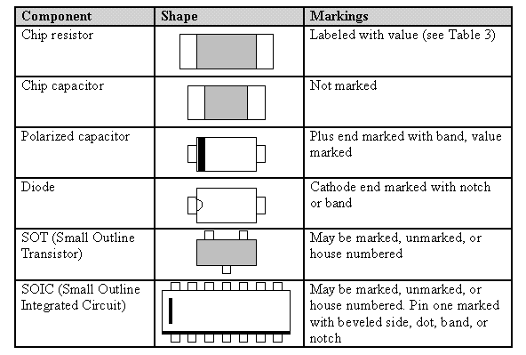
Table 2. Common SMD case sizes.
* This is the most common size for SMD resistors and chip capacitors
Table 3. Typical resistor markings and corresponding values.
SMD transistors are shown in Figure 4 (A) and 4 (B) and are compared to the common T0-92 transistor case style. Notice that the leads for the SOT-23 are totally different than for the TO-92.
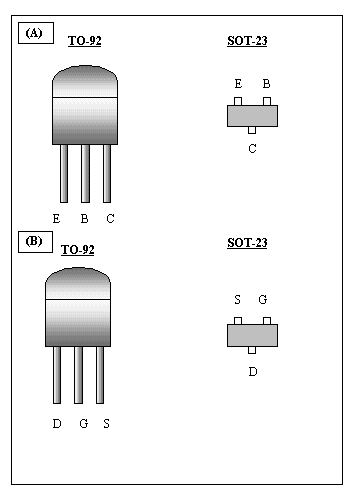
Figure 4. (A) Comparison between a TO-92 bipolar transistor and its surface mount counterpart. (B) Comparison between a TO-92 field effect transistor and its surface mount counterpart.
Removing Individual SMDs
SMDs can be removed using special soldering stations employing custom desoldering tips or hot air jets. If these are not available, you can (with a little practice) remove components using desoldering braid and flux.
To remove an SMD that is already mounted to a circuit board, you will need a roll of fresh desoldering braid and RMA (rosin, mildly activated) flux (liquid or paste). Desoldering braid oxidizes over time, so if it looks dull, replace it.
Infiltrate about one inch of the desoldering braid with flux (if it didn’t come that way). Lay the braid over the solder joint and gently press down with the tip of a soldering pencil. The solder will wick into the braid. Each area of braid can only be used once, so trim it after each try. Repeat several times for each solder joint until all solder (except a very thin film) has been removed.
Grip the component with tweezers and gently twist to release the component (don’t pull or you may lift the pads). If the component does not release from the pads, go back and try to remove more solder.
This technique takes practice, so try removing several components from a surplus board before attempting it on an important project.
Soldering SMDs
There are several ways to successfully solder SMD components to a circuit board. Some are easier to learn than others, and some require the use of special materials (like solder paste, which is a mixture of powdered solder and flux) or special equipment (like SMD solder stations).
One of the simplest ways to solder SMDs is to first glue the components in position on a PC board, then solder the connections. The procedure is:
Clean the copper side of the board with a nonconductive abrasive pad until it is shinny. Wipe off any residue with a tissue and denatured alcohol.
Glue the components into position using Duco cement. Apply the cement to the end of a toothpick, then use the toothpick to apply a drop of cement to the circuit board. Do not get any glue on the pads or any place where you want the solder to flow.
Using self-locking tweezers, position the components on the board. Let the adhesive dry.
Gently nudge the components sideways with a toothpick. If the component moves, try gluing it again.
Apply RMA type paste flux to the component terminals and pads using a toothpick. Apply the flux where you want solder to flow. The function of the flux is to conduct heat from the soldering tip uniformly to the pad and component. The flux also removes surface oxides, which can prevent solder wetting.
Touch the soldering tip (set to about 600 oF) TO THE PAD. Never apply heat directly to the component (it may crack).
Apply small diameter 63/37 solder (0.020" works well) to the pad adjacent to the component terminal. The solder will flow to the component and will form a fillet between the component and pad.
Let the solder cool and remove the flux with denatured alcohol. Inspect with a 4x watchmakers loupe or magnifying glass. The solder joint should be a concave fillet, bright and mirror smooth with no pits as shown in Figure 5.
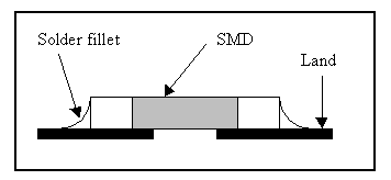
Figure 5. A good solder joint will have smooth, concave fillets as shown in this side view.
Conclusion
Working with SMDs can be challenging, and mastering this technology takes a little patience and practice. Like the transition from point-to-point wiring to printed circuit boards, it is similar to traditional through-hole technology but requires some new skills.
uthor's Bio
Dean F. Poeth II, 218 Gower Rd., Schenectady, NY 12302 holds MS and Ph.D. engineering degrees from The Pennsylvania State University and a BS from The Ohio State University. He is a registered professional engineer in Ohio and a member of the National Engineering Honors Society (Tau Beta Pi), Industrial Engineering Honors Society (Alpha Pi Mu) and Honors Society (Phi Kappa Phi). Dean works at Lockheed Martin in Schenectady, New York. He holds extra class amateur radio and general radiotelephone licenses.
This revised and updated paper originally appeared in the April 2003 issue of CQ magazine.


Komentar ini telah dihapus oleh pengarang.
BalasHapusReally i nice Blog post. Thanks For Sharing this technical blogpost. It's Really helpful. Anybody wants to but PCBA Board may follow:
BalasHapusPCBA Board
Hi, such a nice article when I am searching about the surface mount technology market. I reached on your website you have such a nice and helpful content.
BalasHapus